Introduction
The increasing importance of effective power and supply integrity
management for Nanoprocessors and other ULSI designs has been
well documented recently. Yield loss and timing problems undetected
by traditional verification and validation methods can be traced
to a significant decrease in supply noise margin in components
using advanced fabrication processes at and below the 90nm node.
A combination of increased current density at lower supply voltages
and supply pathway impedance results in large, on and off chip,
relative supply variations called voltage droops in the literature
[1]. These fluctuations make it more difficult to reduce static
and dynamic power and energy consumption by further reductions in supply
voltage, despite the scaling direction for semiconductors. Simultaneously,
finer dimension nanometer processes (90nm and below) exhibit
very substantial device property variances in manufacturing, necessitating
a greater allocation of design margin to such variations.
Therefore, the traditional process-voltage-temperature (PVT)
validation methodology that accorded as much as +/- 10% variance
to supply voltage in the past is now moving rapidly toward more
stringent supply voltage control and lesser voltage variance
tolerance. This trend requires that the combination of DC (static)
and AC (dynamic) noise on-chip be contained within a narrower
supply variance band of +/- 5% or lower in chips in the Nanotechnology
era (100nm to 1nm).
Traditional techniques to minimize supply noise such as voltage
positioning and on-chip decoupling capacitor integration are
seen to become increasingly inapplicable in addressing power
integrity needs. A voltage regulator module (VRM) is far too distant,
both physically and electrically, to match the power supply bandwidth
requirement of gigahertz processors for which the voltage positioning
technique is usually employed. Due to the exponential rise of
gate leakage in sub 100nm processes, on-chip decoupling is seen
to be an unacceptable choice for dynamic noise mitigation. And,
in any case, energy stored in these integrated capacitors diminishes
quadratically with supply voltage. It has also been shown in
the art that the scaling of package filter component characteristics,
such as the loop inductance of on-package capacitors, and the
series resistance of the power path, will be impractically exponential
[Ref. 1, Power Delivery section]. In this paper, we introduce
techniques of active noise regulation (ANR) and active VLSI packaging
(AVP) developed at ComLSI. These methods take advantage of proximity
to the load component and quadratic increase in stored capacitive
energy with voltage to place stable charge reservoirs
where they are most needed, Very close to the high current density
and high-speed, transient loads.
A key requirement in ensuring effectiveness of this technology
is a rigorous understanding of dynamic noise behavior in a high-performance
ULSI component power grid. Tools analyzing the full stack of
multiple on-chip power grids, distributed loads, leakage, and
decoupling capacitance, that also include the package grid, external
connectivity and on-package components are critical for this
understanding. Such tools give the designer the ability to visualize
the spatial and temporal variation of noise throughout the system,
providing a detailed view of the interaction of on-chip dynamic
noise with critical path activity. In addition, these tools provide
a dynamic view of the noise minimization impact of ANR and other
on-package active/passive components. They provide the means
to carefully design the placement and temporal activation of
ANR's, passive decoupling caps and other components in single
or multi-chip systems. True dynamic noise analysis requires the
ability to model all key elements of a power grid including power
loop inductance for all segments of the power grid, on and off
chip standing wave resonances and resistive energy loss. The
authors have made extensive use of such a tool, PI-FP, developed
for this rigorous analysis of dynamic noise in high-performance
systems.
ANR
Active Noise Regulation is a non-disruptive Sysytem-in-Package technology that
addresses power integrity for high-performance ULSI systems and
components such as microprocessors, SoC's, SiP's and multi-chip
assemblies. High-performance, high-power components undergo very
frequent transitions in operational state through a number of
different 'power states' so as to minimize power consumption
while maintaining required performance. These state transitions
occur when applications are running on a processor, and may induce
very sudden, and large swings in power supply current requirement,
exciting the power delivery network into resonance while simultaneously
depleting the local charge stored in the vicinity of the high-bandwidth
load. ANR's address this problem through rapid, controlled and
local supply of charge into the load component power grid. Figure
1 illustrates the implementation of an ANR component shown simply
as a FET switch device. The ANR is associated with a dedicated
'Reservoir' capacitor that is either fed by a supply line connecting
to an external, high-voltage power supply or is charge-pumped
as determined by the system design. This provices the ANR with
a resevoir of charge that is many times greater than charge stored
at the load component's operating voltage.
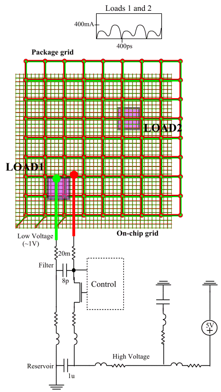 Figure 1: Illustrative Schematic
of an ANR Component Implementation (patent pending)
Figure 1: Illustrative Schematic
of an ANR Component Implementation (patent pending)
In this paper, we discuss and illustrate the impact an ANR
has on a high-performance chip power grid. The ANR (or an array
of ANR's) connects to the load component by very short lengths
of interconnect as in figure 6. The ANR is therefore fully cognizant
of the spatial and temporal variation of the load component power
supply voltages. When the ANR detects (or is intimated of) a
substantial change (say a voltage droop event) in the conditions
at the load component power grid point or region to which it
is connected, it initiates compensating flow of charge from the
Reservoir Cap into the load power grid. After a brief duration
of high current and charge flow, the ANR shuts the current flow
in a controlled manner, allowing the Reservoir Cap to be replenished
and prepared for another such transient event.

Figure 2: Simulation results using a distributed
model on the use of an ANR in a high speed system. The plot shows
the supply voltage change delta(Vdd-Vss) at all points across
the chip surface.
Figure 2 displays simulation results on the use of ANR in
a high speed system with load1 and load2 currents as shown in
figure 1. The animation shows the response of the system's power
delivery stack to a power state transition. This simulation is
carried out in a distributed model that emulates the on-chip
grid and all components of the power delivery system. Various
downward excursions of the grid differential supply voltage are
seen, and are referred to as 'droops'. These droops reduce the
voltage available to the circuits within the chip regions they
occur in and impede their ability to perform required functions
at the chip's operational frequency.
The load on the right hand side of the plot operates without
the benefit of an ANR device. The left hand side of the plot
shows the grid response to an identical load current with ANR
functionality included. For the duration that the ANR component
is active, it may be seen that the voltage droop, or performance-degrading
noise, is reduced substantially. Figure 3 shows the change in
supply voltage at two locations on the on-chip grid close to
the center of each load.

Figure 3: Load current induced power noise
with and without ANR at single points on the chip surface. This
ANR has a filter that tunes the device to the lower frequency
system level transients that occur when blocks are switched on
and off during power saving mode changes.
It is evident from these results that this ANR device is particularly
effective at controlling low frequency system level transients.
While droops have been specifically inspected, ANR's can just
as effectively address overshoots. Low frequency droops and overshoots
are related to supply path inductances and capacitors on-package
and on system boards and is often the most important power noise
component impacting performance in high speed systems. ANR devices
can be employed to reduce noise amplitudes throughout the frequency
range. In figre 4, trace (a) is connected to the package grid close to the ANR
circuit and trace (b) is located near the load without active noise regulation.
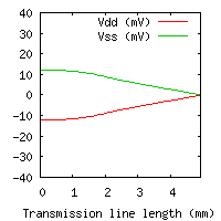 (a)
(a) |
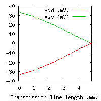 (b)
(b) |
Figure 4: Distributed Vdd and Vss supply
variations along two transmission lines.
Leakage and voltage dependence of dynamic noise
Consideration of the spectral content of power noise is important
in the trade-off between speed and power in the system. Figure
5 shows a simplified model of the system power grid.
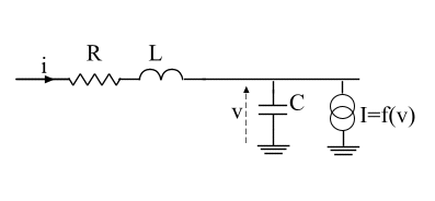 Figure 5: Simple power grid model.
In this model the voltage drop at the load is given by:

where:
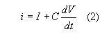
Substituting (2) into (1) gives:

In general, the load current I is a non-linear function of
the power noise v and equation (3) has to be solved numerically.
However, we can gain some insight into the performance of a typical
power grid using quasi-static approximations for the load current.
For example, today's advanced processes have considerably higher
static leakage than previous process generations. This leakage
falls off rapidly during dynamic voltage drops providing negative
feedback that acts to reduce the overall noise level. Substituting
the first order approximation to the system load current (linear
increase in transistor leakage with supply voltage):
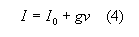
into equation (3), where Io and v are slowly varying
functions of time, gives:

or:

Thus a large static leakage component can provide an overall
reduction in system noise. However, relying on the damping effect
of static leakage also means an acceptance that the system power
consumption will be much higher than it needs to be. And, in
any case, even with a large static leakage contribution to the
overall power consumption, the instantaneous peak dynamic current
density within any particular region of the IC is likely to be
much larger than the static current per unit area at this location.
Note that this feedback will be negative whenever the leakage
current increases monotonically with voltage (e.g. mosfets).
This ensures that the last two terms in equation (3) remain greater
than or equal to zero at all times.
At higher frequencies the remaining terms in equation (3)
can no longer be ignored. Suppose we now switch off the load
current. The power noise can then be written as:
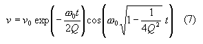
Where vo is the noise level at switch off (t=0)
and


In power networks with Q>0.5 the grid continues to oscillate
for approximately Q cycles after the noise source has been switched
off. The system Q depends on the ratio of the energy stored in
L and C to the energy dissipated in R. In systems designed for
efficient power delivery (high Q), a larger proportion of the
noise energy generated in one cycle remains in the grid during
subsequent cycles. This energy is available to power active loads
in the IC. However, low dissipation systems also have much greater
dynamic voltage drops, particularly at frequencies around the
resonant frequency wo. Any efforts made by designers
to reduce power loss such as the use of low leakage processes
and circuit design techniques will inevitably lead to an increase
in dynamic noise. ANR provides designers with the means to reduce
this noise at higher system speeds without excessive heat generation.
Using ANR the system Q is increased, not by reducing resistance,
but by taking advantage of the quadratic increase in capacitive
energy with voltage to place large amounts of energy at the load.
The advantages of low loss power transport at high voltage, followed
by voltage conversion at the load, have been well known since
the early days of power distribution. This advantage can now
be realised for high-speed systems using ANR.
AVP
A severe limitation in the capability of on-chip capacitors
in storing charge follows from the relationship:

where charge and capacitance are per unit area and E is the
electric field in the charge storage device. The maximum capacitance
per unit area integrated within chips is typically in a MOS-capacitor.
Most fabrication processes push the MOS capacitor dimension (gate
oxide thickness) to being fine enough that the reliability limit
for the gate oxide is approached. Therefore it is not feasible
to store greater charge per unit-area (and energy) within an
integrated MOS capacitor using higher voltage, since high-voltage
tolerant devices within the fabrication process must necessarily
have a thicker gate oxide, thereby reducing their capacitance
per unit area approximately in proportion to the higher voltage
desired.
The importance of package capacitors has been amply demonstrated
in experiments conducted at a high-volume microprocessor manufacturer
that showed that in the presence of even one land-side package
capacitor, the quantum of on-die capacitance integrated did not
seem to matter to component performance (maximum frequency).
Land-side package capacitors are mounted on the opposite side
of the processor package substrate and immediately below it such
that the physical thickness of the package substrate separates
the capacitor from the processor circuits. This is one of the
closest practical assemblies of capacitors and large values of
stored charge to a processor both from a physical and an electrical
standpoint. In other words, integrated on-chip capacitance may
be too far laterally and therefore, electrically, to be of as
much value in mitigating noise as much as properly positioned
package capacitors. Package capacitors are therefore seen to
be more effective in maintaining processor power integrity.
In other experiments, it has been demonstrated that removing
many of the package capacitors while retaining an appropriately
placed few also seemed to have little impact on the performance
of the processor. This result indicates the importance of understanding
the exact spatial and temporal nature of dynamic noise in a chip
grid; a package capacitor at a location of low dynamic noise,
or a location where dynamic noise does not coincide with a critical
circuit or circuit path on the die may not be of significant
benefit in optimal power integrity management.
A key limitation of passive devices such as package capacitors
is that they are 'reactive' devices. In other words, they react
to changing electrical conditions around them. A capacitor therefore
only provides charge flow when there is a substantial rate of
change of voltage across its terminals. Therefore, while a capacitor
serves as a reservoir of electric charge, it cannot pro-actively
provide copious amounts of charge to suppress a sudden or transient
voltage variation. It only supplies charge when it encounters
a substantial voltage variation or droop.
Additionally, the effective series resistance (ESR) and inductance
(ESL) of these capacitors is fixed in value, and while manufacturing
and device design improvements reduce the value of these parasitic
elements, that is not necessarily advantageous. While lower ESR
values assist in minimizing the voltage and power dropped within
the capacitor as it supplies charge, low ESR does not effectively
damp supply grid oscillations excited by the switched nature
of the load. Passive devices therefore do not provide mechanisms
to assist in the suppression of resonant power supply voltage
variations.
In Active VLSI Packaging, package capacitors are combined
with land-side mounted ANR devices (figure 6). These structures
locate the high voltage reservoir capacitor and control circuitry
within a distance of a package substrate thickness of the processor
or SoC die. The ANR device makes use of the large energy capacity
of these reservoirs to pro-actively restore charge to the on-die
power grid. This technique thus allows active control of dynamic
power noise with minimal power consumption. Additionally, active
noise regulators provide a means for introducing dynamic damping
impedances into a chip power delivery system, pro-actively controlling
supply resonances.

Figure 6: ANR and LVR devices can be package
or PCB mounted. This ensures a low impedance, minimal delay path
to the high performance IC (patent pending).
The natural evolution of ANR's is into local voltage regulators
(LVR's) that provide extremely high-bandwidth, on-package, high-efficiency
power conversion. LVR's use the parasitic elements associated
with package capacitors and the supply pathways into the chip
power grid to provide extremely high frequency switched power
conversion. An array of LVR's augment the externally supplied
low voltage power supply and dramatically increase the bandwidth
of the full power delivery system. This allows a high-power SoC
component to rapidly modulate the supply voltage provided to
it's circuits in order to minimize average power supply consumption.
The proximity of LVR's tothe load component enables fast communication
between the SoC and the LVR array, thereby enabling the rapid
transitions in supply voltage and the significant power consumption
reduction that results from dynamic energy management.
Conclusion
System level simulation methods have shown that active noise
regulation can be used to control noise in low loss power grids.
These tools and design methodologies allow system designers increased
flexibility when designing low noise, high speed systems with
minimal power consumption. In addition, the authors believe a
package for a chip can do a lot more than provide interconnect
pathways for power and signal connections. It is increasingly
clear in RF and high-speed design that package components provide
high-performance passives that enhance the performance of integrated
circuits. Packaging for RFID components captures energy to power
the circuits. Given the proximity to the integrated circuits,
package components will soon function actively and symbiotically
with SoC chips, providing efficient, cost-effective systems solutions
to power and signal integrity management. ANR and LVR devices
and arrays are capable of non-disruptive change in the established
integrated circuit and system packaging architectures addressing
power integrity and management. Electronic circuit and systems
packaging will play an 'active' role in system function and performance
to push integration further in the Nanotechnology era.
[1] R. Mahajan, Raj Nair et al., "Emerging
Directions for Packaging Technologies", ITJ '02. |