Introduction
How do advanced design changes impact power integrity? This is a question often encountered by power-integrity aware IP block designers.
And here is where a front-end analysis environment such as Anasim's PI-FP is most useful. We introduced PI-FP's key characteristics in a prior publication years ago [1].
There, we described how a true physical simulation environment assists chip floor planning. We looked at on-chip capacitor allocation and explored active noise regulation.
In this example, we look at load current modulation.
Clock edges in a synchronous IC tend to display large supply current spikes.
These spikes are a load to the local power grid and result in significant droop or dynamic voltage drop. Designers often wonder if they may use advanced techniques,
such as intentional clock skew, to alter such loads. The technique has much intuitive appeal: distribute gate switching to reduce supply load coincidence.
In this simple example, we look at one such modification to a clock domain and its PI impact.
Clock-edge current load is split in two by a partitioned clock domain and designed clock skew. Supply current consumption is "spread out" in time,
and we look at PI degradation for both cases. What do we expect to see? What can we learn about differences between PI-FP and a non-physical IR Drop simulation?
Power Grid and Load Block
Figure 1 below shows a chip power grid connecting through package pathways to a supply point.
The load block connects to the power grid within an area bounded by supply connections. Abstract power bus information, such as bus widths and separation,
defines the grid. Electrical information relevant to PI, such as Inductance, Capacitance, and Resistance, are also captured. Note, as a floor planning environment,
that PI-FP captures key circuit physical aspects.
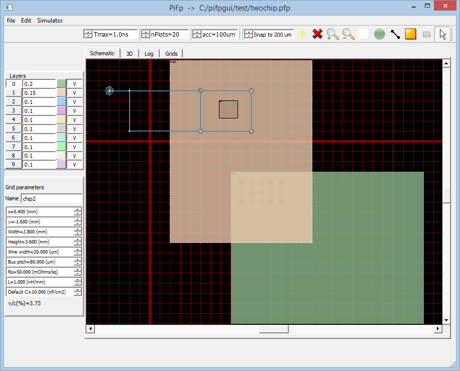 Figure 1: Physical schematic of power grid and load block in PI-FP
Figure 2 shows load block physical and electrical aspects captured in PI-FP. Note a 'v/c' fraction in both schematic views.
This represents a check for physicality: speed of EM wave propagation in the grid. Any power grid without inductance violates this law of physics.
Resistive grids beat c, the speed of light (no matter what tool vendors tell you)!
 Figure 2: Load block (block1) physical and electrical aspects
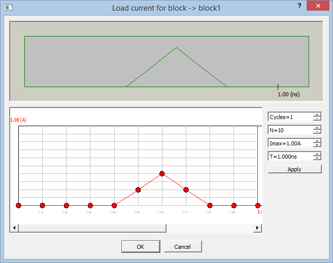 Figure 3: Single peak block load current.
Let's first look at a load condition where logic circuits switch with a single clock edge.
The supply current spike is a single triangular load peak as seen in Figure 3. Clock skew and jitter produce anything from a Gaussian to a Bathtub
distribution of edges in time. But this approximation suffices for our simple 'what-if' analysis. Figure 3 illustrates the load current peaking at 0.6ns.
PI-FP permits easy manipulation of block load current waveforms in the GUI popup shown.
A quick simulation run takes only a few seconds for this simple experiment.
3D visualization of grid noise indicates voltage droop of about 120mv. Dynamic supply noise peaks at 0.6ns as seen in Figure 4.
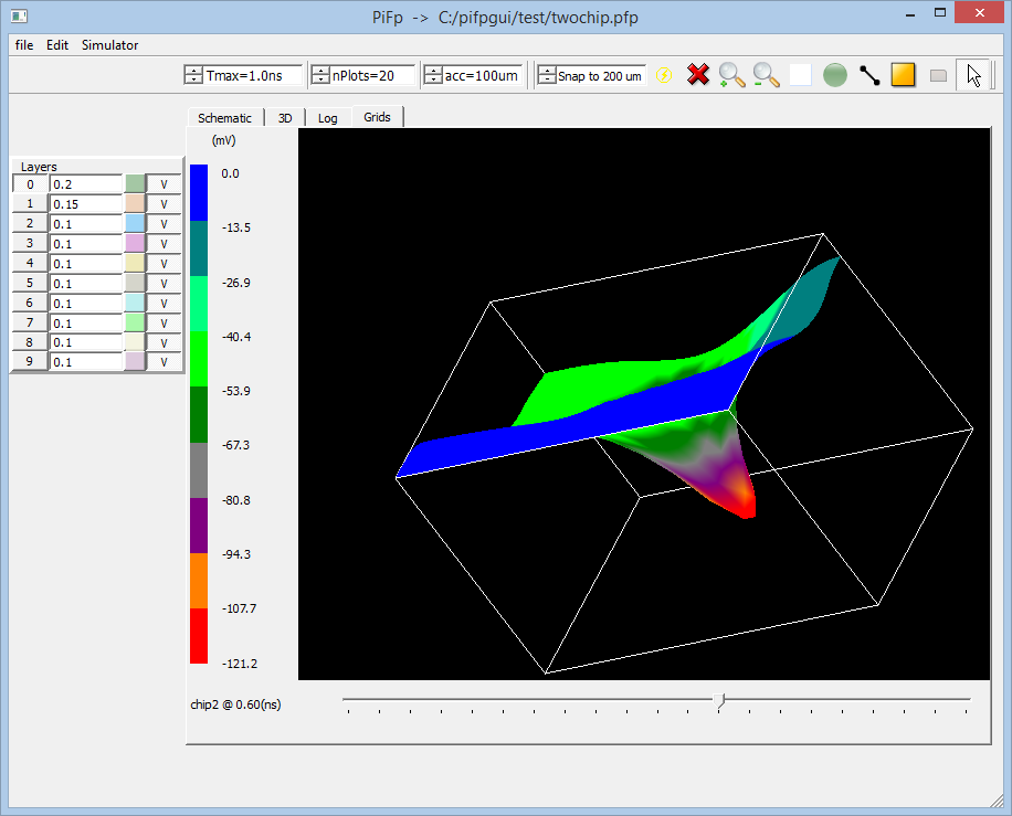 Figure 4: Grid noise with a single peak block load current.
Next, we change the load current (in PI-FP's GUI) waveform to a dual-peak shape.
This approximates for a partition of the block into two clock domains, with clock edges skewed by 200ps between them. Note, in this instance,
that edge placement variability has halved. A rough guesstimate for a divided clock domain. This may not always be the case, of course.
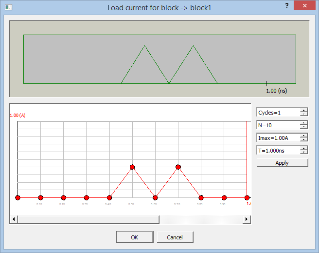 Figure 5: Supply current in a partitioned clock domain with intentional clock skew.
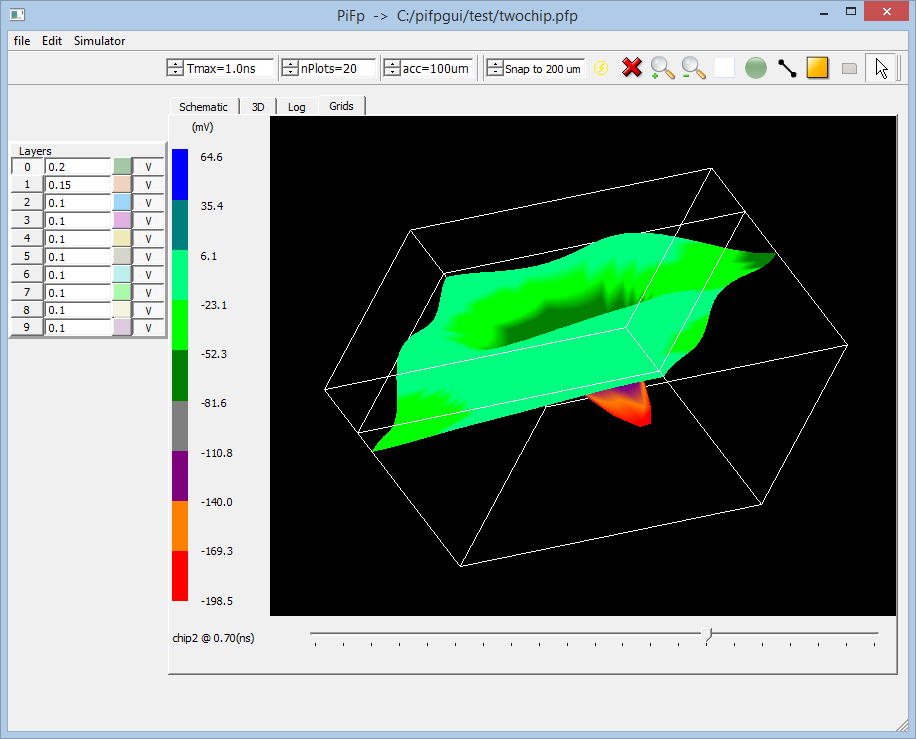 Figure 6: Grid noise with a partitioned clock domain and intentional clock skew.
Discussion: Load peaks, di/dt, and Rogue Wave nature of dynamic voltage droop
The results are startling, are they not? What had we hoped for? Diminished power grid noise, given that lesser numbers of logic gates switched together.
But we see a noise peak of about 200mv, ~ 66% higher, coincident with the second supply current peak at 0.7ns. Just how did this occur in our simple experiment?
It's clear that we must revisit our experimental assumptions and setup.
And there's where we find our first possible error. We shrank the time base of the load current peaks since fewer gates switched together.
The physical proximity of circuits in each partition must diminish edge timing variability. But wait - we did not account for fewer gates in each domain
switching at identical times! Shouldn't the peaks thus be smaller than in the single peak case?
But Euclidean (or Cartesian, if you like) mathematics is of little help to us. Supply current consumption is charge drawn from the supply and transferred
into switching circuits. The area under any load current wave represents this charge quantity. The two load scenarios must hence display the same load current
wave area. Two half-base triangles must have the same height to equal one full-base wave.
Perhaps it'll help if we reduce designed skew from 200ps (20% of the clock period) down to say 100ps. But wouldn't that overlap the two waves?
And increase the number of circuits switching together? Another what-if experiment!
As constructed, our experiment does provide some insight. The dual-peak load waveform displays higher di/dt and can increase grid noise.
This is especially true where inductance to nearby decoupling is significant. Two adjacent load peaks in a single block can lead to constructive noise interference.
This is the most likely reason for noise peaking at 0.7ns, the instance of the second load current peak. We demonstrated and documented this, albeit with spatially separated loads, in early 2008 [2]. The results may be counterintuitive, but not inexplicable.
Our assumptions - that feed intuition - may need revision.
Summary
First: Homage to the infallible GIGO principle. You know - garbage in, garbage out! It is important that input stimuli reflect actual circuit behavior.
Second: A simulation environment that ignores grid inductance ignores true grid impedance. Results in such non-physical simulations cannot reflect grid impedance
variation with load spectrum changes. You get no local L*di/dt if you have no local L. Third: Resistive grids do not propagate waves with any accuracy. RC models filter out high-frequency waves.
No rogue waves or local grid resonances in such approximations. Besides, with peak-i*r calculating noise, what difference will you see between the two cases?
Especially - if you do get the dual load peaks to be smaller? Again, the simulation environment, if non-physical, cannot sign-off on physical verification!
This experiment was created and run in PI-FP, and took only a few minutes. A true-physical 'what-if' environment greatly enhances early design exploration. For more on PI-FP, or such experiments, please contact us.
|


